A Trusted partner with a service model ideal for custom process integration for a range of technology leaders
Since the creation of our Minnesota site’s custom foundry business in 2013, we’ve partnered with innovators to co-create disruptive and highly differentiated process technologies for imaging, sensing, genetic sequencing, quantum computing and numerous other applications. We offer comprehensive integration expertise that spans MEMS, photonics, CMOS and PICs for monolithic or wafer-level integrations. Our TaaS engagement model is geared to engage customer ideas as early as MRL 3 and accelerate bespoke or highly differentiated process integrations to production to address high quality markets including medical, automotive and industrial among others.
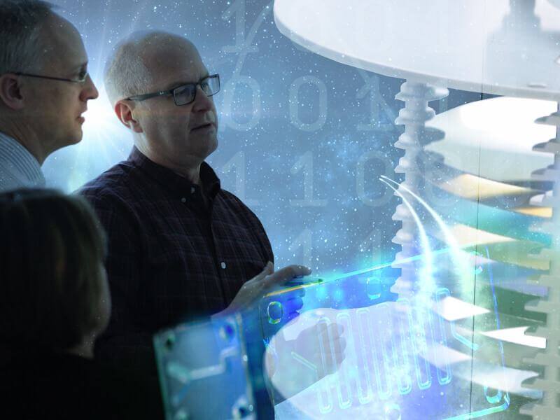
Our TaaS model co-creates custom architectures that leverage our integration expertise for various device types
SkyWater is the pioneer of the Technology as a Service model and specializes in streamlining new ideas from concept to production. This is an ideal engagement model for MEMS, photonics and emerging technologies that require custom process integration.
Technology as a Service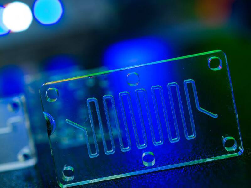
MEMS capabilities to enable numerous device types
- Actuators, micro-motors
- Biosensors and microfluidics
- CMUTs
- Gas/chemical sensors
- Infrared detectors: microbolometers, thermopoiles
- Micro-speaker, electrostatic
- Pressure sensors
- Resonators
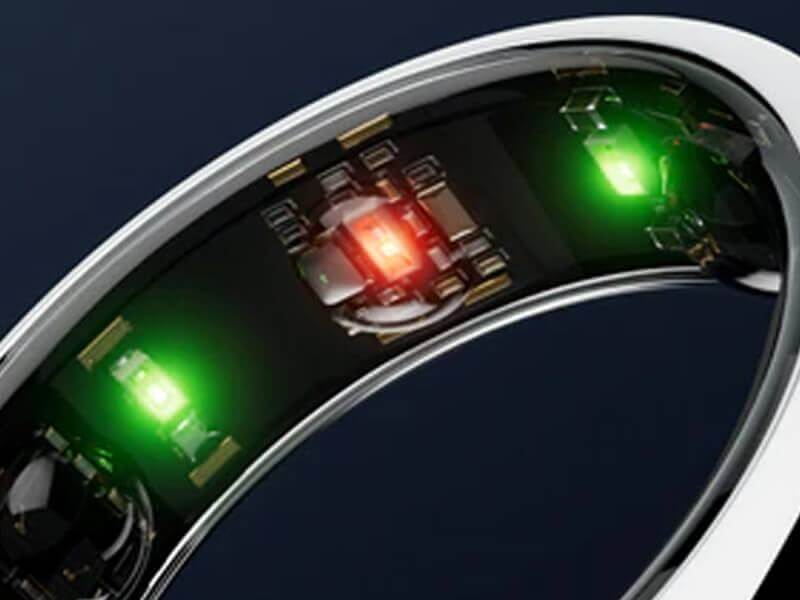
Co-creating with SkyWater is more than great optics
Photonics and optical device development at SkyWater’s U.S. investor-owned facilities means leveraging our automotive quality legacy to accelerate your path to market in an IP-secure environment.
- Detectors
- Fiber couplers
- Grating couplers
- Modulators
- Waveguides
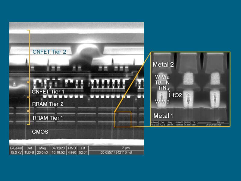
CMOS platforms for hybrid integrations with smart sensors
Automotive-grade 90 nm and 130 nm Silicon CMOS technologies and CNFET based SoCs enable unique monolithic architecture solutions.
Rich processing modules enable differentiated technologies
MEMS, Photonics & Custom Process Integration Capabilities
See a comprehensive list of integration capabilities at our Facilities & Capabilities page.
| Capability | Tool | Comment |
|---|---|---|
| Deposition and etch for Au, Nb | AMAT Endura PVD | |
| Pt deposition, others possible | Evatec Evaporator | |
| Dense features, fine pitch | ASML 1400XT | 55 nm capable (single pattern): high aspect ratio waveguides, gratings, nano/micro channels |
| High AR TSVs and trenches | SPTS Rapier | Bosch process |
| Thick Cu plating and TSV fill | Semsysco Triton | |
| Polyimide ILD and Release | DNS Coat | |
| CMP of Si, Ge, Nb, Al, Cu | AMAT Mirra | Multiple slurry systems |
| ALD of HfO2, Al2O3, TiN | ASM Pulsar | |
| AlN deposition | Endura | Superconducting |
| Wafer-wafer bonding | SUSS XBS200 | |
| Fine pitch lift-off patterning | Veeco Storm |
Critical quality systems for high-value markets
Integration expertise ideal for MEMS architectures
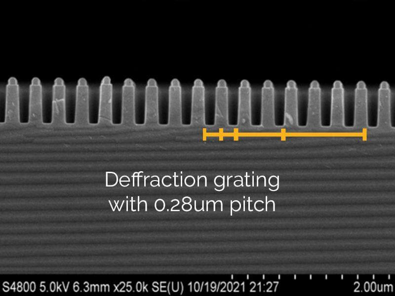
Photonics with High Aspect Ratio Features
- Diffraction grating with 0.28um pitch

MEMS Fine Features & CDs
- 40 nm fluidic nanochannels
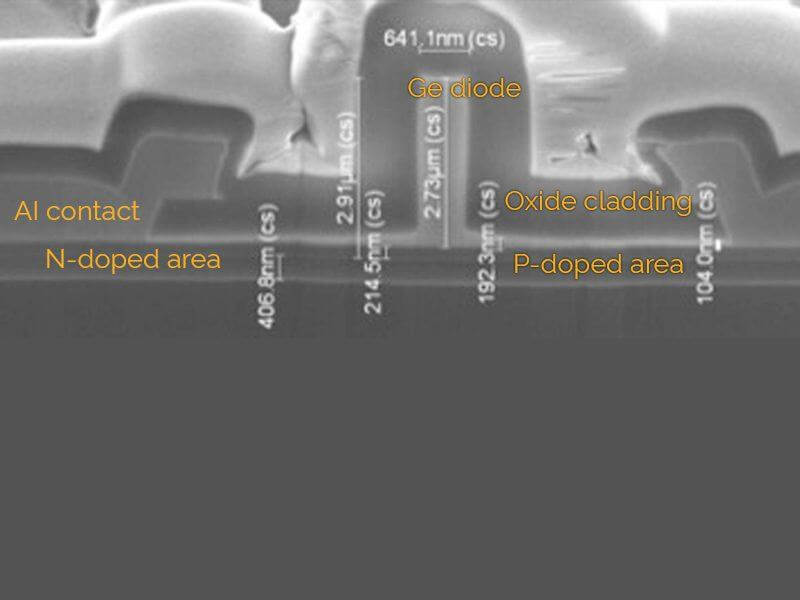
Conformal Films

CMOS Platforms for Hybrid Integration and Heterogenous Integration Services
- Silicon interposers
- W2W oxide and hybrid bonding
- Roadmap for fine pitch FOWLP integration

